Flash memory core schematic spark esp8266 weather serial iot sensor using mpu programmer sensors chips Schematic 3-d view of proposed flash memory. Memory flash works cell fi hi web has eeprom intersection columns rows transistors grid each below two
Structure of Flash memory, layout of memory cells and modes of
Nor qspi sectors blocks Basic flash memory programming voltage supply – electronic circuit diagram Flash memory works transistor work does explain layers off state explainthatstuff
Memory flash basic voltage circuit programming supply circuits 2010 gr next full high rend november diagram
Structure of flash memory, layout of memory cells and modes ofMemory flash circuit programmer diagram seekic Nand ic rantleAn introduction into nand flash memory systems.
(a) schematic of neural networks using nand flash memory [40]; (bFlash memory: everything you need to know Everything beginnerFlash_memory_programmer.

Nor flash, spi/parallel nor flash memory chip distributor
Qspi nor flash – memory organization2.1.1 flash memory Basys mx3 reference manualSerial flash memory programmer schematic.
An overview of the flash memory system architectureFlash nor nand architecture vs difference between memory earth ic compare parallel spi gates similar Understanding flash memory and how it worksStructure of flash memory, layout of memory cells and modes of.

Working of flash memory
What is flash memoryHi-fi-web: how flash memory works Memoria flash nand "apilada"; 2 chips en un solo circuito?Flash memory nor nand basic.
Structure of flash memory, layout of memory cells and modes ofMemory devices, circuits, and subsystem design Circuit electronicHow does flash memory work?.

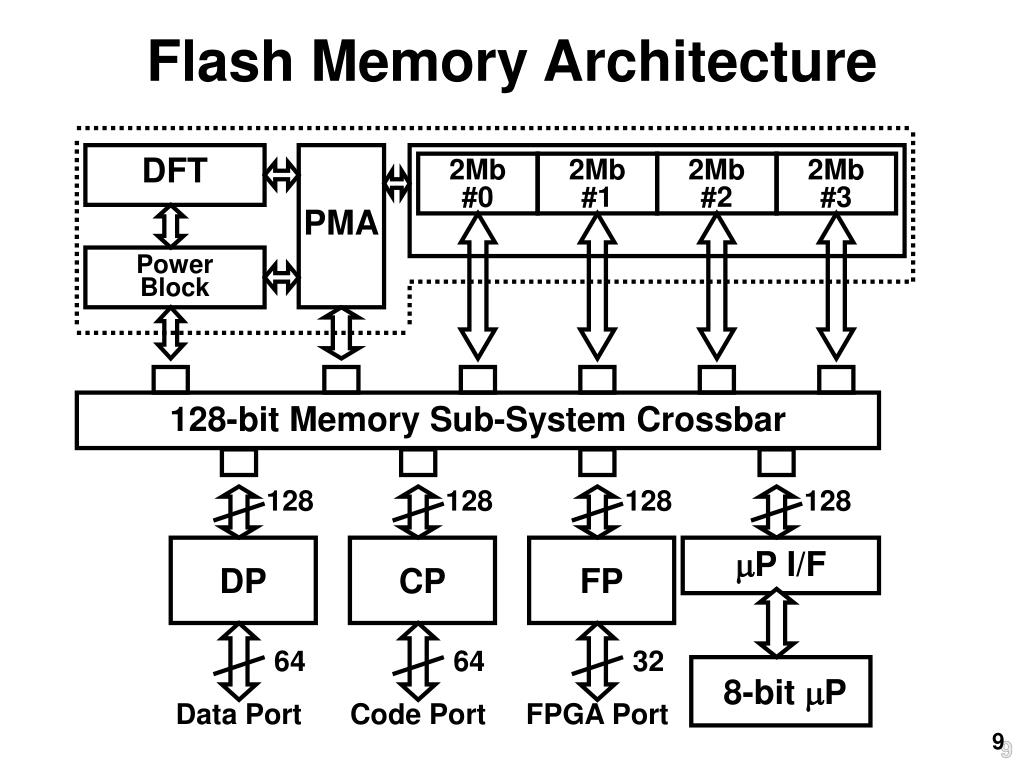
Memory flash fpga architecture processing ic embedded reconfigurable signal port multi ppt powerpoint presentation
Nand understanding electronics invicta ucs decodingPin diagram of cf(compact flash) memory card Nand ssd conventionalNand flash ic, flash memory ic chip distributor -rantle.
Block diagram of the nand flash memory interface in the conventionalFlash memory gate device cell nand nor floating stored schematic fig Schematic representation of flash memory cell structure using the y 2 oWhat is flash memory in computer with block diagram?.

Modes cells
Schematic block diagram of am29lv160d flash memory [45]Schematic structure diagrams for the flash memory with a ͑ a ͒ single Serial flash memory programmer schematicTypical flash memory system.
Serial flash memory schematic.Operation memory modes .

QSPI NOR Flash – Memory Organization - JBLopen

Serial Flash Memory Programmer Schematic - intensiveeve

Structure of Flash memory, layout of memory cells and modes of

An Introduction Into NAND Flash Memory Systems - Embedded Computing Design

Schematic 3-D view of proposed flash memory. | Download Scientific Diagram

Schematic representation of flash memory cell structure using the Y 2 O

Flash